Networks
I - Lab Section 3: Mondays
Lab Assignment 3 - due:
next Monday 2 October 2006
Lab 3 – Resistive Circuits, Node-Voltage and
Mesh-Current
Objectives: The objective of this lab is to use different circuit analysis methods to solve simple resistor circuits. The Node-Voltage Method and the Mesh-Current Method will be used and compared on the same circuit. A third circuit will be designed and built via Mentorgraphics to simulate an Analog to Digital Converter.
Procedure:
Part 1:
Build the circuit below using four different resistors. When building the circuit, select resistor values such that the power generated in each resistor in the circuit will be well below its ¼ Watt power dissipation rating. This will involve doing some calculations first.
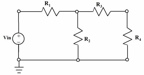
Select four different resistances for R1, R2, R3, R4 and a DC input voltage Vin. Using the Node-Voltage Method, (Ohm’s Law and KCL) write down the equations to solve this circuit. Select the four resistors with the power consideration mentioned above and build the circuit using those resistors. Next, using the Mesh-Current Method, (Ohm’s Law and KVL) write down the equations to solve the circuit. Using the selected resistors from above, solve the equations to get all the currents in the circuit. Measure the currents and voltages throughout the circuit using the multi-meter and compare them to the results from both methods. Explain any differences in the results. Explain when one method would be used over another.
Part 2:
A client asks you to build a circuit to power the backlight of an LCD display. The load resistance of the display is 1.1 kΩ and needs 2mA to operate. You have 5 volts available to you from other circuitry. Design and build a circuit that will power the backlight of the LCD display. Explain your approach and each step you took in your design process. Measure the electrical parameters of your circuit and make sure they comply with your design. Explain your results.
Part 3:
Design a Digital to Analog Converter Circuit. A Digital to Analog Converter accepts a binary signal and converts it to an equivalent analog value. Look, for instance, at a four bit binary number as shown in Table 1.
Table 1
|
Binary # |
1 |
0 |
1 |
1 |
|
|
Power of 2 |
23 |
22 |
21 |
20 |
|
|
Decimal Equiv. |
8 |
0 |
2 |
1 |
= 11 |
Each of the binary bits is the equivalent of an identical voltage source that is either "on" (full voltage) or "off" (ground or zero volts). Your lab assignment is to design and build (via Mentorgraphics) a resistive circuit that contains 4 identical voltage supplies (bits) (V1, V2, V3, V4) where full voltage is 5 volts and has an output (OUT) that scales as follows:
Table 2
|
V1 |
0 |
5 |
0 |
5 |
0 |
5 |
0 |
5 |
0 |
5 |
0 |
5 |
0 |
5 |
0 |
5 |
|
V2 |
0 |
0 |
5 |
5 |
0 |
0 |
5 |
5 |
0 |
0 |
5 |
5 |
0 |
0 |
5 |
5 |
|
V3 |
0 |
0 |
0 |
0 |
5 |
5 |
5 |
5 |
0 |
0 |
0 |
0 |
5 |
5 |
5 |
5 |
|
V4 |
0 |
0 |
0 |
0 |
0 |
0 |
0 |
0 |
5 |
5 |
5 |
5 |
5 |
5 |
5 |
5 |
|
OUT |
0 |
0.1 |
0.2 |
0.3 |
0.4 |
0.5 |
0.6 |
0.7 |
0.8 |
0.9 |
1.0 |
1.1 |
1.2 |
1.3 |
1.4 |
1.5 |
Your lab report should include a description of how you used the steps of the problem-solving method that is shown in your text in Figure 1.7-1 (page 18). Print out a schematic of your final circuit and simulation verification for each of the four cases that are shown in bold type in Table 2. (above)