Homework Given January 30, 2007
Due February 6, 2007
This assignment is due on
Live Links to the Exercises
![]() Exercise 1.65
(FET transistor simplified circuits)
Exercise 1.65
(FET transistor simplified circuits)
![]() Exercise 2.7
(Norton equivalent circuit for output of op-amp)
Exercise 2.7
(Norton equivalent circuit for output of op-amp)
Exercise 1.37
Prove that a resistor is a linear circuit element…
Show that ![]() using Kirchhoff’s laws
and Ohm’s law.
using Kirchhoff’s laws
and Ohm’s law.
Exercise 1.51
Find the Thévenin equivalent of the circuit of Figure P1.2
and show the role of resistor ![]() . Figure P1.2 is on
page 28.
. Figure P1.2 is on
page 28.
The open circuit voltage is determined by ![]() and
and ![]() as a voltage divider,
and the source voltage of 12 V. The
short circuit current is determined by
as a voltage divider,
and the source voltage of 12 V. The
short circuit current is determined by ![]() and the source
voltage. The role of
and the source
voltage. The role of ![]() is to load the source
with a current but
is to load the source
with a current but ![]() does not affect the
Thévenin equivalent at the terminals a and a’.
does not affect the
Thévenin equivalent at the terminals a and a’.
Exercise 1.65 (FET transistor simplified circuits)
Find the Thévenin equivalents of each of the circuits (a),
(b), and (c) of figure P1.65, using the test source method to find the Thévenin
equivalent resistance. For each of the
three circuits, we will determine the open circuit voltage to obtain the
Thevenin voltage, then, we modify the circuit to make the Thevenin voltage zero
by setting ![]() to zero and use the
test source method to find the Thevenin resistance. We set
to zero and use the
test source method to find the Thevenin resistance. We set ![]() to zero and apply a
test voltage
to zero and apply a
test voltage ![]() to terminals
to terminals ![]() and
and ![]() and solve the circuit
for the current out of the test source to find the Thevenin resistance.
and solve the circuit
for the current out of the test source to find the Thevenin resistance.
Part (a)
Here, ![]() is a voltage drop
across a resistance
is a voltage drop
across a resistance ![]() . Note that the
designation
. Note that the
designation ![]() is used twice in this circuit We will
modify the problem to avoid confusion by designating the first one
is used twice in this circuit We will
modify the problem to avoid confusion by designating the first one ![]() . There is a voltage
divider that determines
. There is a voltage
divider that determines ![]() ,
,
![]() .
.
Given ![]() , we used the controlled source and Ohm's law to find the
Thevenin equivalent voltage as
, we used the controlled source and Ohm's law to find the
Thevenin equivalent voltage as
![]() .
.
We see from the circuit that the test source does not cause
a voltage across ![]() so the controlled
current is zero amperes. This the
Thevenin equivalent resistance is
so the controlled
current is zero amperes. This the
Thevenin equivalent resistance is ![]() ,
,
![]() .
.
Part (b)
This circuit is simplified by making ![]() and open circuit and
adding a resistor
and open circuit and
adding a resistor ![]() to what would be an
emitter resistor in a bipolar transistor.
The voltage
to what would be an
emitter resistor in a bipolar transistor.
The voltage ![]() that drives the
controlled source is the difference between
that drives the
controlled source is the difference between ![]() and the voltage drop across
and the voltage drop across ![]() , which we find by Ohm's law to be
, which we find by Ohm's law to be
![]() .
.
This gives us an equation for ![]() ,
,
![]()
which we solve as
![]() .
.
We again use Ohm's law to find the Thevenin equivalent voltage,
![]() .
.
For ![]() equal to zero, the
output is the same as for part (a), so the Thevenin equivalent resistance is
the same,
equal to zero, the
output is the same as for part (a), so the Thevenin equivalent resistance is
the same,
![]() .
.
Part (c)
Here we have the same circuit as part (b), but the problem
statement is to find the Thevenin equivalent for the terminals across ![]() . Since the circuit is
the same as for part (b), we can use the results from part (b) to find
. Since the circuit is
the same as for part (b), we can use the results from part (b) to find ![]() and thus the
controlled current, which we use with Ohm's Law to find the Thevenin controlled
voltage,
and thus the
controlled current, which we use with Ohm's Law to find the Thevenin controlled
voltage,

We note that setting ![]() to zero leaves the
ungrounded terminal of
to zero leaves the
ungrounded terminal of ![]() connected to an open
circuit, but unlike part (b) the test source will have an effect on
connected to an open
circuit, but unlike part (b) the test source will have an effect on ![]() ,
,
![]() .
.
The current out of the test source will be the draw through ![]() by Ohm's law minus the
current from the controlled source,
by Ohm's law minus the
current from the controlled source,

so the Thevenin equivalent resistance is
![]() .
.
Exercise 1.99
Find the relationships between the resistances and capacitances for a voltage divider as shown in Figure P1.99 on page 35, both of whose impedances are a resistor in parallel with a capacitor.
The impedance of a resistor and a capacitor in parallel is
 .
.
The circuit in the figure is a voltage divider of two such impedances. Any of several methods will show that the ratio of the resistances must be the inverse of the ratio of the capacitances. I suggest writing the voltage divider equation for the two impedances and finding a relationship for the transfer function, e.g. the voltage divider output voltage divided by the input voltage in terms of the two impedances,
Any one of the last three forms given here suggest that the transfer function is independent of frequency when
![]()
or, the ratios of the resistances and capacitances are the inverse of each other,
![]() .
.
The problem statement points out that the circuit is similar
to that of an oscilloscope probe. The input, ![]() , is the voltage under test.
The top resistance,
, is the voltage under test.
The top resistance, ![]() , is a high resistance such as
, is a high resistance such as ![]() to offer minimum
effect on the circuit under test. The
top capacitance
to offer minimum
effect on the circuit under test. The
top capacitance ![]() is the stray
capacitance in the probe tip resistance, with a value such as
is the stray
capacitance in the probe tip resistance, with a value such as
![]() .
.
The resistance ![]() is the oscilloscope
impedance, which is typically
is the oscilloscope
impedance, which is typically ![]() . Note that
resistances of
. Note that
resistances of ![]() in the probe and
in the probe and ![]() in the oscilloscope
are typical of a 10X probe, and at DC and low frequencies, the oscilloscope
will see 1/10 of the voltage under test.
in the oscilloscope
are typical of a 10X probe, and at DC and low frequencies, the oscilloscope
will see 1/10 of the voltage under test.
The capacitor ![]() must be 10 times the
stray capacitance
must be 10 times the
stray capacitance ![]() for the oscilloscope
to see 1/10 of the voltage under test at high frequency. If the high frequency response isn't the same
as the low frequency response, not only will the oscilloscope be out of
calibration at high frequencies, the waveforms that it displays will be
distorted. Thus there is a trimmer
capacitor that adjusts
for the oscilloscope
to see 1/10 of the voltage under test at high frequency. If the high frequency response isn't the same
as the low frequency response, not only will the oscilloscope be out of
calibration at high frequencies, the waveforms that it displays will be
distorted. Thus there is a trimmer
capacitor that adjusts ![]() in the jack of the
oscilloscope probe where it plugs into the oscilloscope, and a typical trimmed
value of this capacitance is
in the jack of the
oscilloscope probe where it plugs into the oscilloscope, and a typical trimmed
value of this capacitance is ![]() .
.
Exercise 2.6
In the simple op-amp model shown in Figure 2.2 on page 39, current may flow either direction through the output terminal. In a real op-amp, from where do these currents come?
If you look at the general block diagram of an op-amp shown on page 37, which I also drew on the board in class on more than one occasion, the output stage of an op-amp is a follower amplifier. The currents that it provides come from the power supplies.
Exercise 2.7 (Norton equivalent circuit for output of op-amp)
Draw the dual of the op-amp of figure 2.2, with Norton equivalent output driven by the input current between the inverting and non-inverting input.
Ohm's law gives the input current as
![]()
and we have the Norton equivalent current of the output as
![]() .
.
The Norton equivalent resistance is the same as the Thevenin
equivalent resistance, ![]() . We can use these
equations together to eliminate
. We can use these
equations together to eliminate ![]() and find
and find
![]()
to give us the Norton equivalent circuit for the output, in terms of the current between the terminals in the input.
Exercise 2.19
A vacuum sensor provides a resistance that varies from ![]() to
to ![]() as the vacuum varies
from atmospheric pressure to 10-3 torr. Design a circuit that provides a voltage that
uses this variable resistance to vary its output from 0 V to 10 V. Voltages available are -12 V, 0 V (ground),
and +12 V. Use standard 5% resistor
values.
as the vacuum varies
from atmospheric pressure to 10-3 torr. Design a circuit that provides a voltage that
uses this variable resistance to vary its output from 0 V to 10 V. Voltages available are -12 V, 0 V (ground),
and +12 V. Use standard 5% resistor
values.
The Preface of our text, on page vi, states that homework problems marked with a script "D" as does 2.19 have significant design content. As noted at the top of the page where the homework problems begin, such as page 87, the problems are marked according to level of effort required: no marking is easiest, an open circle requires more effort, a half-filled circle is harder, and a filled circle denotes the most difficult category. Problem 2.19 is marked with an open circle. This, problem 2.19 requires that you formulate a circuit – the part of the problem where you need to design – and you will need to refer to the book and give it a little thought – hence the open circle marking.
The first clue is that 2.19 falls in a block of problems involving non-inverting amplifiers as treated in section 2.4.1, pages 41 through 43. Thus you can reasonably expect that there is a non-inverting amplifier in a simple circuit that will solve the problem. So, part of your circuit will look like Figure 2.5 on page 41.
The rest of our problem states that we have a sensor that
provides a resistance that varies from ![]() to
to ![]() , and that an output is desired that varies from 0 Volts to
10 Volts as the resistance varies over that range. The op-amp must drive a
, and that an output is desired that varies from 0 Volts to
10 Volts as the resistance varies over that range. The op-amp must drive a ![]() load, which is no
problem with any general purpose op-amp.
We have
load, which is no
problem with any general purpose op-amp.
We have ![]() and
and ![]() available for the sensor circuitry and to power the op-amp.
available for the sensor circuitry and to power the op-amp.
A last requirement is that we use 5% standard value
resistors. In the Index on page 1123,
under "Resistor color code/standard values," Appendix D on pages
1097-1099 is listed. A table on page
1099 lists standard resistor values for 5%, 10%, and 20% tolerances over the
range 10 to 91. Note that "22"
means any of ![]() ,
, ![]() ,
, ![]() ,
, ![]() ,
, ![]() etc. are standard 5%
values. The text of Appendix D and table
D.1 show that the color code of any one of these resistors will be red, red, a
multiplier value, and gold to indicate 5% tolerance, so colored bands beginning
at one end will have these colors. The
multiplier color will be black for
etc. are standard 5%
values. The text of Appendix D and table
D.1 show that the color code of any one of these resistors will be red, red, a
multiplier value, and gold to indicate 5% tolerance, so colored bands beginning
at one end will have these colors. The
multiplier color will be black for ![]() , brown for
, brown for ![]() , red for
, red for ![]() , etc.
, etc.
We now have enough information to block out our design
problem. We need to place our variable resistor
in a simple circuit with one or two other fixed standard value resistors. Voltages available to apply to this circuit are ![]() , 0 Volts (ground), and
, 0 Volts (ground), and ![]() . We want a node on
this circuit to provide 0 Volts when the resistor is
. We want a node on
this circuit to provide 0 Volts when the resistor is ![]() and a positive voltage
when the resistor is
and a positive voltage
when the resistor is ![]() , and this voltage is to be provided to the non-inverting
input of the op-amp in the circuit on page 41.
Note that, for an ideal op-amp, there is no current being drawn from our
sensor circuit, which simplifies the design and analysis of the sensor circuit.
, and this voltage is to be provided to the non-inverting
input of the op-amp in the circuit on page 41.
Note that, for an ideal op-amp, there is no current being drawn from our
sensor circuit, which simplifies the design and analysis of the sensor circuit.
We now have reduced our problem to answering three questions:
- What
is the simplest possible circuit that includes our variable resistor and
hooks to two of the voltages
 , ground or 0 Volts, and
  that produces 0
Volts when our variable resistor is
that produces 0
Volts when our variable resistor is  and a positive
voltage when our variable resistor is
and a positive
voltage when our variable resistor is  ? Can we do this
with only one other fixed resistor?
Is this resistor a standard 5% value -- listed in the 5% column of
the table on page 1099, times a power of 10?
? Can we do this
with only one other fixed resistor?
Is this resistor a standard 5% value -- listed in the 5% column of
the table on page 1099, times a power of 10? - The
non-inverting amplifier will give us 0 Volts when the sensor resistor
circuit gives us 0 Volts. What is
the gain required to give an output of 10 Volts from the non-inverting
amplifier when the sensor resistor is
 ?
? - The
gain of a non-inverting amplifier is
 as given in
Figure 2.5 on page 41, the discussion and equation (2.6) on the top of
page 42, Example 2.1 on page 42, and equation (2.12) on page 43. What is a ratio of standard 5% values
from the table on page 1099 that gives us the closest possible gain we
need according to step 2? We use
those values, with an appropriate multiplier -- power of ten -- to keep
the resistors in the range of
as given in
Figure 2.5 on page 41, the discussion and equation (2.6) on the top of
page 42, Example 2.1 on page 42, and equation (2.12) on page 43. What is a ratio of standard 5% values
from the table on page 1099 that gives us the closest possible gain we
need according to step 2? We use
those values, with an appropriate multiplier -- power of ten -- to keep
the resistors in the range of  to
to  , to complete our design.
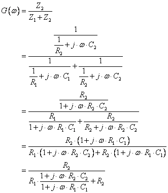
The simplest possible circuit is a voltage divider. A voltage divider that produces zero volts
must have a positive and a negative voltage, so we have two resistors connected
to the ![]() and
and ![]() voltage sources. We need zero volts when the sensor resistor
voltage sources. We need zero volts when the sensor resistor ![]() has a value of
has a value of ![]() , so the added resistor has a fixed value of
, so the added resistor has a fixed value of ![]() . We will be using a
non-inverting op-amp configuration by direction, so the voltage divider must
provide a positive voltage when
. We will be using a
non-inverting op-amp configuration by direction, so the voltage divider must
provide a positive voltage when ![]() takes a value of
takes a value of ![]() , so
, so ![]() is connected to the
is connected to the ![]() voltage source.
voltage source.
The output of the voltage divider is

so when ![]() takes on the value of
takes on the value of ![]() , we have
, we have ![]() at the output of the
voltage divider. The non-inverting
amplifier must provide a gain of 2.5 to provide an
at the output of the
voltage divider. The non-inverting
amplifier must provide a gain of 2.5 to provide an ![]() of
of ![]() from an input of
from an input of ![]() . From Section 2.4.1
and Figure 2.5 on page 41, we see that the gain of the non-inverting op-amp
circuit is
. From Section 2.4.1
and Figure 2.5 on page 41, we see that the gain of the non-inverting op-amp
circuit is ![]() , so we need a ratio of 1.5 to 1 for
, so we need a ratio of 1.5 to 1 for ![]() . From Table D.2 on
page 1099, we see that 10 and 15 are standard values for 5% resistors, so we
pick
. From Table D.2 on
page 1099, we see that 10 and 15 are standard values for 5% resistors, so we
pick ![]() and
and ![]() as convenient
values. The final circuit is shown below
in Figure 1. The equation
for the output voltage as a function of the sensor resistance is
as convenient
values. The final circuit is shown below
in Figure 1. The equation
for the output voltage as a function of the sensor resistance is
![]()
which is seen to meet the
requirements of a voltage swing from 0 V to ![]() as
as ![]() increases from
increases from ![]() to
to ![]() . The final
requirement, that the circuit drive a
. The final
requirement, that the circuit drive a ![]() load, is met by using
an op-amp output as the circuit output.
load, is met by using
an op-amp output as the circuit output.
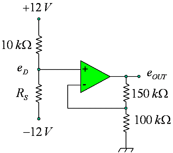
Figure 1 Design for Problem 2.19