Biasing of BJT Inverting Amplifiers and Emitter Followers
Navigation
![]() Kirchhoff's Current Law with Node Voltage
Notation
Kirchhoff's Current Law with Node Voltage
Notation
![]() The Circuit Voltages and Currents
The Circuit Voltages and Currents
![]() The Thévenin or Norton Equivalent Circuits for the
Emitter and Collector
The Thévenin or Norton Equivalent Circuits for the
Emitter and Collector
![]() The Norton Equivalent for the Collector of a BJT
Inverting Amplifier
The Norton Equivalent for the Collector of a BJT
Inverting Amplifier
![]() The Thévenin Equivalent for the Emitter of a
BJT Emitter Follower
The Thévenin Equivalent for the Emitter of a
BJT Emitter Follower
![]() Inverting Amplifier Voltage Gain
Inverting Amplifier Voltage Gain
![]() Robustness of the Design for Varying Current Gain for
Different Bias Circuits
Robustness of the Design for Varying Current Gain for
Different Bias Circuits
![]() Designing an Inverting Amplifier Stage
Designing an Inverting Amplifier Stage
The Base Circuit
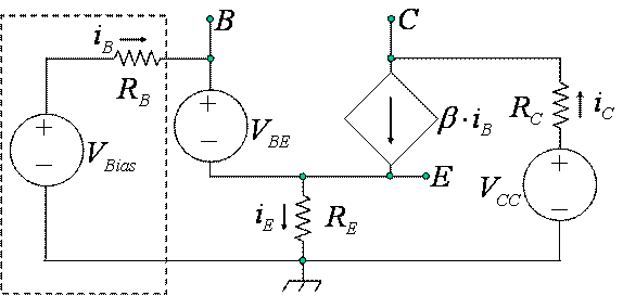
Figure
1. Simple Transistor Model with Resistive Loads and
Bias Circuit.
The circuit shown in Error!
Reference source not found. is a simplified model of a bipolar
junction transistor (BJT). The portion
of the circuit inside the dotted rectangle is a Thévenin equivalent circuit of
the biasing circuit. The base, emitter,
and collector terminals are denoted by ![]() ,
, ![]() , and
, and ![]() respectively. The base-emitter diode junction is modeled by
a constant voltage drop, the source
respectively. The base-emitter diode junction is modeled by
a constant voltage drop, the source ![]() , which for most silicon transistors is about 0.6 Volts.
, which for most silicon transistors is about 0.6 Volts.
A typical v-i curve for a BJT is shown in Error! Reference source not found.. The transistor model used in Error! Reference source not found. applies for the transistor operating between cutoff and saturation. The purpose of the bias circuit is to provide an operating point for which the model is valid. The operating point must be far enough from saturation and cutoff so that signals of magnitude for which the circuit is designed will not cause the transistor to be in saturation or cutoff during part of the waveform.
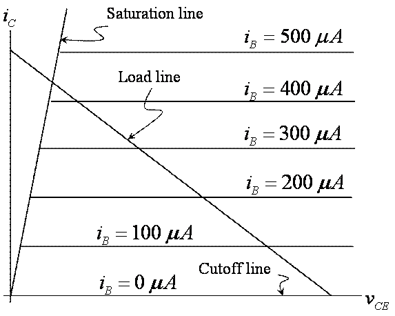
Figure
2. Idealized v-i
Curves and Load Line for a BJT Transistor.
Solving the Circuit
Kirchhoff's Current Law with Node Voltage Notation
The nodes in the circuit of Error! Reference source not
found.are the base, emitter, and collector nodes. These are denoted on the schematic by ![]() ,
, ![]() and
and ![]() , respectively. Note
that the emitter and base are a supernode when the constant voltage drop model
is used for the base-emitter diode. The
node equations are
, respectively. Note
that the emitter and base are a supernode when the constant voltage drop model
is used for the base-emitter diode. The
node equations are
![]()
Ohm's law equations for the base, emitter, and collector currents are
Substituting the Ohm's law forms for the currents into the KCL equations

Putting these equations into matrix form gives us
 .
.
Note that the top row has no dependence on the collector
voltage ![]() . This is because the current
source presents infinite impedance between the collector model and the emitter
and base portion of this simple transistor model. As a result, we can solve for the emitter
voltage
. This is because the current
source presents infinite impedance between the collector model and the emitter
and base portion of this simple transistor model. As a result, we can solve for the emitter
voltage ![]() directly and use it in
the equation for the collector circuit to find the collector voltage
directly and use it in
the equation for the collector circuit to find the collector voltage ![]() .
.
The Circuit Voltages and Currents
Now we solve for the emitter voltage ![]()
and the collector voltage ![]()
The base current is found by Ohm's law as
We substitute ![]() from into and obtain
from into and obtain
![]()
This circuit is similar to those considered in Example 1.3, pages 10-12, and homework problem 1.65 on page 33. The principal difference is that the transistor model in Figure 1Error! Reference source not found. models the base-emitter junction as a voltage drop rather than a resistance. The effective dynamic resistance of the base-emitter junction is modeled here as part of the Thévenin resistance in the bias circuit.
Looking at the components connected to the emitter using the
KCL, the emitter current ![]() is the sum of the base
current
is the sum of the base
current ![]() and the collector
current
and the collector
current ![]() . Since, in this
idealized transistor model, the collector current is the current gain
. Since, in this
idealized transistor model, the collector current is the current gain ![]() times the base
current, we have
times the base
current, we have

With the base current ![]() we have the collector
current
we have the collector
current ![]() as
as
![]()
The v-i curves of the transistor are for the collector-emitter voltage, which we find from and to be
![]() .
.
The load line is a straight line on the v=i curve that
reflects the Thévenin equivalent circuit made up of the supply voltage ![]() and the collector
circuit resistance
and the collector
circuit resistance ![]() . The intercepts on
the v-i plot are the supply voltage
. The intercepts on
the v-i plot are the supply voltage ![]() on the voltage axis
and
on the voltage axis
and ![]() on the current axis.
on the current axis.
The circuit can operate as a linear amplifier only when the operating point is on the load line in a region between saturation and cutoff.
An important addition to the load line is a curve of allowable power dissipation for the transistor. This is a hyperbola with asymptotes of the v and i axes, and the region between this curve and the axes represents the allowable operating region for the transistor without exceeding the power dissipation specified. The equation for the allowed region is
and is an important part of the design process. The load line can cross this curve and part of the operation of the transistor may be outside the allowable region, but the quiescent (zero signal) operating point must be in the allowed region.
The Thévenin or Norton Equivalent Circuits for the Emitter and Collector
The Norton Equivalent for the Collector of a BJT Inverting Amplifier
We have the Thévenin equivalent circuit for the power supply
voltage source ![]() and collector
resistor. There is a Norton equivalent
circuit for the transistor side of the collector circuit: the controlled current source. The Norton equivalent resistance is the
dynamic collector resistance of the transistor, which we neglect in the simple
transistor model that we are using here.
In an actual transistor, the horizontal lines in the i-v curves for the
transistor at different base currents will have a slight upward slope,
corresponding to a high but finite dynamic collector resistance. Typical values of this parameter for BJTs are
and collector
resistor. There is a Norton equivalent
circuit for the transistor side of the collector circuit: the controlled current source. The Norton equivalent resistance is the
dynamic collector resistance of the transistor, which we neglect in the simple
transistor model that we are using here.
In an actual transistor, the horizontal lines in the i-v curves for the
transistor at different base currents will have a slight upward slope,
corresponding to a high but finite dynamic collector resistance. Typical values of this parameter for BJTs are
![]() to a few megohms.
to a few megohms.
The Thévenin Equivalent for the Emitter of a BJT Emitter Follower
The circuit of Figure
1can be used as a model of an emitter follower by
omitting ![]() and taking its value
as zero in the circuit solution. The
open circuit voltage at the emitter is given by and the short circuit current
is given by taking
and taking its value
as zero in the circuit solution. The
open circuit voltage at the emitter is given by and the short circuit current
is given by taking ![]() as zero in ,
as zero in ,
The Thévenin resistance is the ratio of the open circuit voltage as given by and the short circuit current as given by ,
![]()
An interesting way that the Thévenin resistance can be
viewed is as the parallel combination of the emitter resistance and the base
resistance divided by ![]() ,
,
 .
.
Note that the reciprocals of both Thévenin equivalent resistances are seen as the diagonal terms of the matrix in .
The Voltage Gain for Signals
Inverting Amplifier Voltage Gain
The inverting amplifier voltage gain can be obtained from by noting that a signal added to the bias voltage will result in a signal component in the collector voltage, mapped linearly through the dependence of the collector voltage on the bias voltage. Thus the inverting amplifier voltage gain is
![]()
Note that the emitter resistor ![]() can limit the signal
gain, which can never reach
can limit the signal
gain, which can never reach ![]() . This gain limit can
be incorporated into the design as a way to define gain independently of
. This gain limit can
be incorporated into the design as a way to define gain independently of ![]() or it may be
eliminated, at least partially, by bypassing the emitter resistor with a large
capacitor.
or it may be
eliminated, at least partially, by bypassing the emitter resistor with a large
capacitor.
Emitter Follower Voltage Gain
The emitter follower voltage gain can be obtained from by noting that a signal added to the bias voltage will result in a signal component in the emitter voltage, mapped linearly through the dependence of the emitter voltage on the bias voltage. Thus the emitter follower voltage gain is
![]() .
.
Robustness of the Design for Varying Current Gain for Different Bias Circuits
The principal variation between circuits in production is the
current gain ![]() of the transistor,
which will vary in a sample population far more than the 5% tolerance used for
resistors. We have noted that the
operating point of the transistor must be between saturation and cutoff, and maximum
voltage swing for the output is achieved when the operating point is halfway
between the minimum collector voltage at which the transistor enters the
saturation region, and cutoff, when the collector voltage reaches
of the transistor,
which will vary in a sample population far more than the 5% tolerance used for
resistors. We have noted that the
operating point of the transistor must be between saturation and cutoff, and maximum
voltage swing for the output is achieved when the operating point is halfway
between the minimum collector voltage at which the transistor enters the
saturation region, and cutoff, when the collector voltage reaches ![]() .
.
A simple indicator of how sensitive the design is to
variation in current gain ![]() is the sensitivity of
is the sensitivity of ![]() to
to ![]() , which is
, which is

A good measure of the stability of the circuit is the ratio
of the sensitivity of the output voltage to undesired variation in the current
gain ![]() and desired change in
the output voltage to input signal. This
ratio is
and desired change in
the output voltage to input signal. This
ratio is
Inspection of and shows the rationale for several design principles:
Even a small emitter resistor ![]() can have a dramatic
stabilizing effect on the transistor operating point, particularly for very
high current gain
can have a dramatic
stabilizing effect on the transistor operating point, particularly for very
high current gain ![]() . Since high current
gain is the most common parameter variation between transistors in a lot, this
is a very important design feature.
. Since high current
gain is the most common parameter variation between transistors in a lot, this
is a very important design feature.
Decreasing ![]() will improve stability
in proportion exceeding circuit gain.
This is the reason that most transistors are biased through a voltage
divider from
will improve stability
in proportion exceeding circuit gain.
This is the reason that most transistors are biased through a voltage
divider from ![]() instead of making
instead of making ![]() equal to
equal to ![]() .
.
Keeping the base resistor ![]() small improves
stability. This is another reason to use
a voltage divider from
small improves
stability. This is another reason to use
a voltage divider from ![]() to reduce the value of
to reduce the value of
![]() and thus keep the
required value of resistance for
and thus keep the
required value of resistance for ![]() small.
small.
Since ![]() does not appear in , the choice of collector
resistor
does not appear in , the choice of collector
resistor ![]() does not affect
stability relative to gain.
does not affect
stability relative to gain.
Designing an Inverting Amplifier Stage
Here we will take these parameters as given:
![]() The
supply voltage
The
supply voltage ![]() . Here we will use +12
Volts.
. Here we will use +12
Volts.
![]() The
mean transistor current gain
The
mean transistor current gain ![]() and its expected
range. Here we will use 300, with
tolerances of -50% to +100%.
and its expected
range. Here we will use 300, with
tolerances of -50% to +100%.
![]() The
remainder of the design is directed toward meeting the requirements of the
design. The required performance of the
inverting amplifier will vary with the application. Here we will ask for maximum voltage swing on
output, and low output impedance. The
steps in the design are
The
remainder of the design is directed toward meeting the requirements of the
design. The required performance of the
inverting amplifier will vary with the application. Here we will ask for maximum voltage swing on
output, and low output impedance. The
steps in the design are
![]() Draw
a hyperbola on the v-i plot that shows the maximum power dissipation of the
transistor that you will allow in your design.
This will be below the maximum power dissipation given in the data
sheet, and will reflect heat sinks and any dissipation limitations in your
expected layout, and your design safety factor.
Draw
a hyperbola on the v-i plot that shows the maximum power dissipation of the
transistor that you will allow in your design.
This will be below the maximum power dissipation given in the data
sheet, and will reflect heat sinks and any dissipation limitations in your
expected layout, and your design safety factor.
![]() Find
a first design load line, and thus the collector circuit load resistance
Find
a first design load line, and thus the collector circuit load resistance ![]() . The minimum
resistance, and thus the minimum output impedance, will be tangent to the
parabola that you drew as the locus of maximum allowable power dissipation for
the transistor.
. The minimum
resistance, and thus the minimum output impedance, will be tangent to the
parabola that you drew as the locus of maximum allowable power dissipation for
the transistor.
![]() Select
an operating point on the load line. For
maximum voltage swing, this operating point will be midway between saturation
and cutoff. The operating point defines
a base current from the i-v plots of the transistor, and, with the current gain
Select
an operating point on the load line. For
maximum voltage swing, this operating point will be midway between saturation
and cutoff. The operating point defines
a base current from the i-v plots of the transistor, and, with the current gain
![]() , a base current. This
operating point must satisfy .
, a base current. This
operating point must satisfy .
Experiment
The Circuit
The supply voltage ![]() is 12 Volts.
is 12 Volts.
The design center current gain ![]() is 120.
is 120.
The maximum allowable transistor power is 50 milliwatts, far below the 2N3905 limit of 625 milliwatts.
The gain is to be set to 50, so the ratio of ![]() is set to 50.
is set to 50.
We use a forward voltage drop of the base-emitter junction ![]() of 0.7 Volts.
of 0.7 Volts.
We find that a resistance of 720 Ohms will limit transistor power
to 50 milliwatts with a 12 Volt power supply.
We will use 1000 Ohms for ![]() and 50 Ohms for
and 50 Ohms for ![]() to get our ratio of 50
to 1 to set the gain. We set the
operating point so that the emitter voltage is set properly. With the expected collector current and value
of resistance for the emitter resistor, we find that a bias current of about 60
microamperes is needed for the nominal current gain of the 2N3904. For a base voltage of about 1 volt, a value
of
to get our ratio of 50
to 1 to set the gain. We set the
operating point so that the emitter voltage is set properly. With the expected collector current and value
of resistance for the emitter resistor, we find that a bias current of about 60
microamperes is needed for the nominal current gain of the 2N3904. For a base voltage of about 1 volt, a value
of ![]() of about
of about ![]() is needed for a
is needed for a ![]() of 6 Volts. We begin with a voltage divider of two
of 6 Volts. We begin with a voltage divider of two ![]() resistors, which
offers a Thévenin equivalent voltage of 6 Volts and an equivalent resistance of
resistors, which
offers a Thévenin equivalent voltage of 6 Volts and an equivalent resistance of
![]() . We will vary the
lower resistor as shown in Figure
3 to obtain a collector voltage of about 5 Volts.
. We will vary the
lower resistor as shown in Figure
3 to obtain a collector voltage of about 5 Volts.
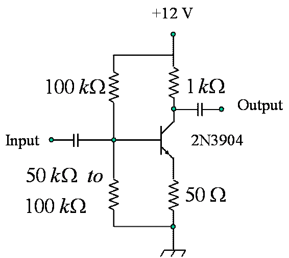
Figure 3. Circuit for BJT Biasing Experiment.
Lab Report Requirements
Your lab report will describe the process used to find the
circuit that you used. Show why a value
of ![]() of
of ![]() is used, what the
maximum possible transistor power dissipation is, give the v-i curve for the
transistor using the simple transistor model presented here, and the load line
for
is used, what the
maximum possible transistor power dissipation is, give the v-i curve for the
transistor using the simple transistor model presented here, and the load line
for ![]() . Show the hyperbola
that bounds the permitted region for an allowed maximum transistor dissipation
of 50 milliwatts. Describe the process
you used to find the final values for the voltage divider in the bias
circuit. Provide measurements of the
voltages on the base and collector.
. Show the hyperbola
that bounds the permitted region for an allowed maximum transistor dissipation
of 50 milliwatts. Describe the process
you used to find the final values for the voltage divider in the bias
circuit. Provide measurements of the
voltages on the base and collector.
Measure the gain of the completed inverting amplifier by adding coupling capacitors as shown in Figure 3 and using your signal generator and oscilloscope. Use a voltage divider on your signal generator output if necessary to provide a small enough signal to provide an undistorted output.
Measure the frequency response of your amplifier by finding the 3 dB rolloff points for the high frequency limit.